Products 레이저 미세가공 서비스
Polymer
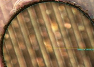
PET Film
Wavelength : 355nm
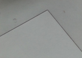
PET Film
Wavelength : 355nm
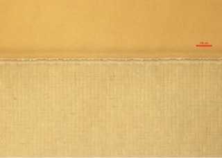
FTO Release (FTO on glass)
Wavelength : 355nm
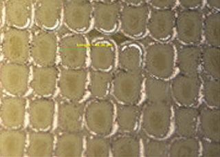
Polyimide Film
Wavelength : 532nm
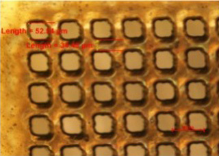
Polyimide Film Cutting
Wavelength : 355nm
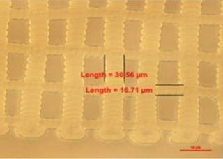
ITO Scribing (Including Ag)
Wavelength : 355nm
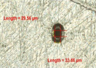
Hole Drilling
Wavelength : 355nm
Thickness : 2.8nm
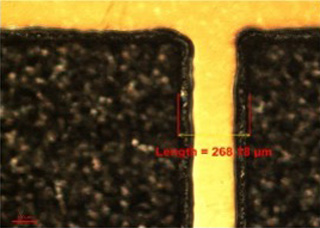
Polaroid Film Patterning
Wavelength : 355nm
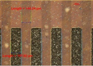
IRO Scribing (Ag Including)
Wavelength : 355nm
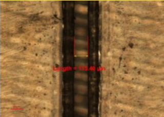
PET Film
Wavelength : 10.6µm
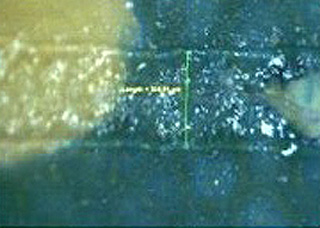
PET Easy Cut
Wavelength : 355nm
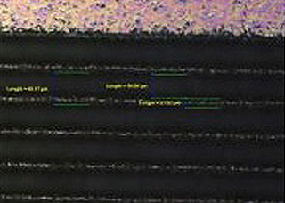
ITO Patterning (on the PET film)
Wavelength : 355nm
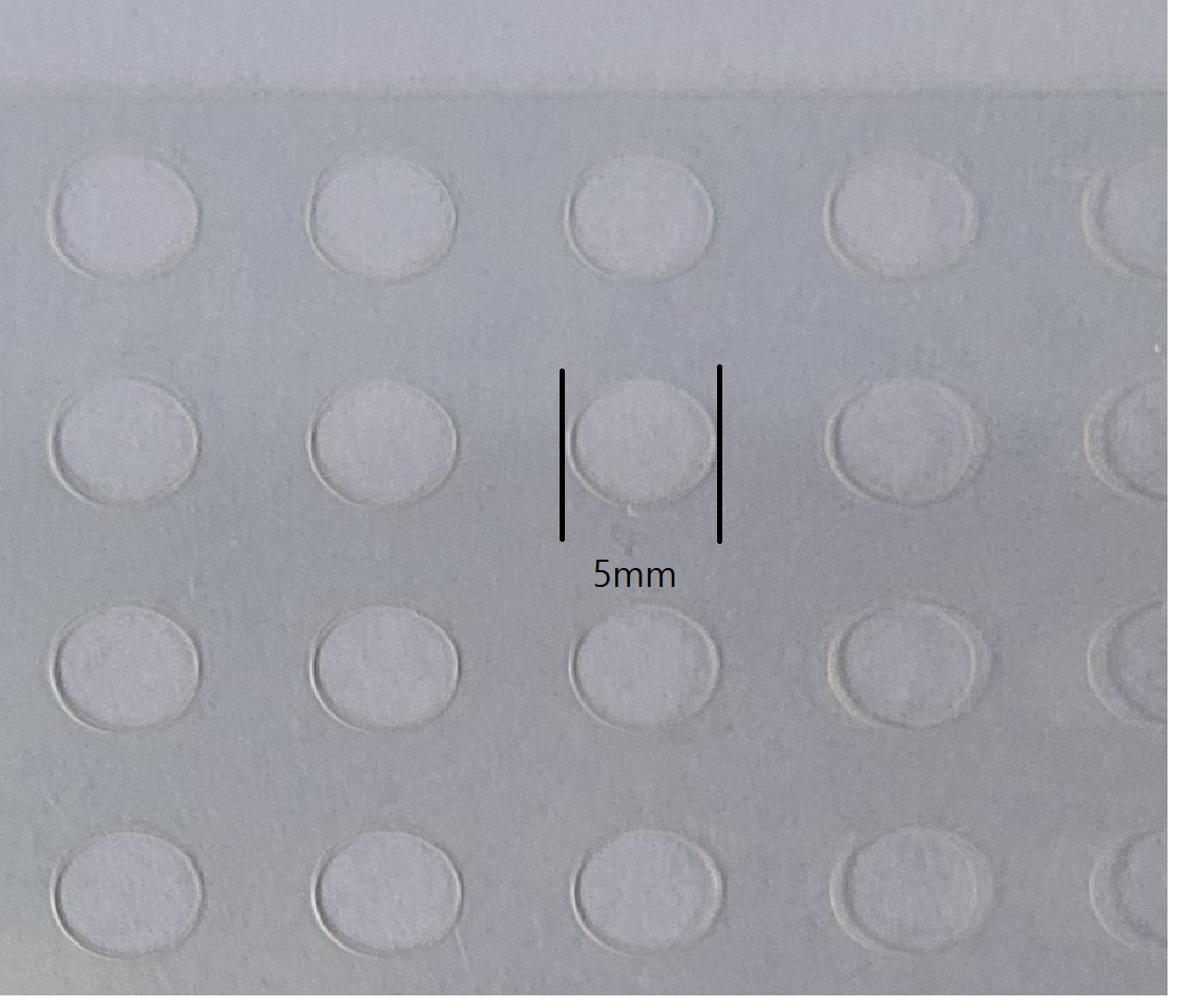
PI Film Circle Cutting
Wavelength : 355nm
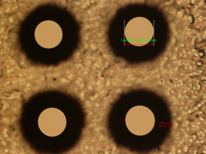
PI Film Circle drilling hole 1
Wavelength : 355nm(Pico seconds laser UV)
Thickness : 300μm
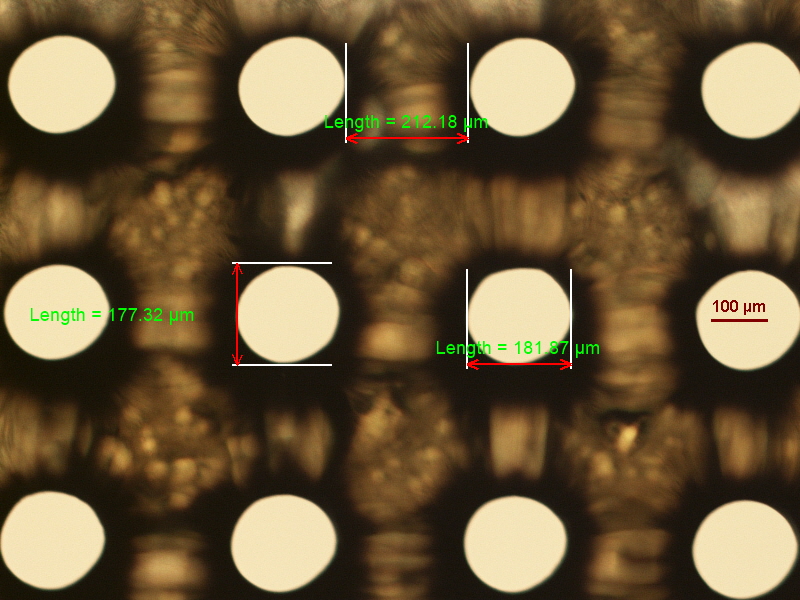
PI Film Circle drilling hole 2
Wavelength : 355nm(Pico seconds laser UV)
Thickness : 300μm
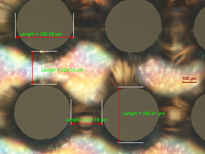
PI Film Circle drilling hole 3
Wavelength : 355nm(Pico seconds laser UV)
Thickness : 300μm
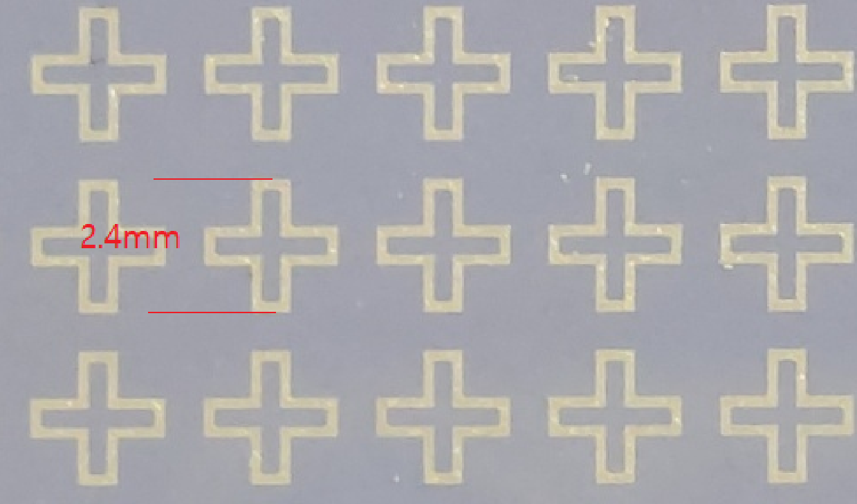
ITO Film Cross Patterning
Wavelength : 355nm
Thickness : 150nm
Wafer
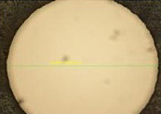
Drilling of Si-Wafer
Wavelength : 1064nm
Pulse energy :
Rep rate : 10kHz
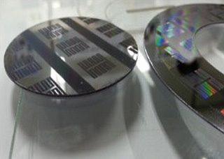
Si Wafer Round Cutting
Wavelength : 532nm
Thickness : 520μm
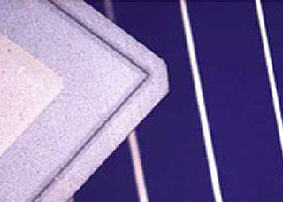
Edge Isolation of Si Solarcell
Wavelength : 1064nm
Pulse energy :
Rep rate : 500kHz
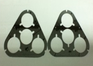
Si Wafer Pattern Cutting
Wavelength : 532nm
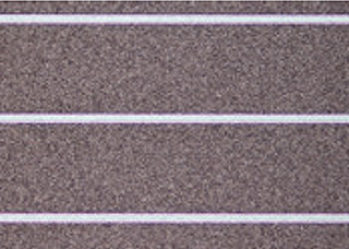
Removal of TCO on CIGS + Mo Glass
Wavelength : 1064nm
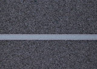
Removal of CIGS on Mo+Glass
Wavelength : 1064nm
Pulse energy :
Rep rate : 500kHz
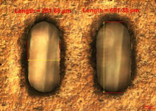
Silicone Sheet Hole Drilling
Wavelength : 355nm
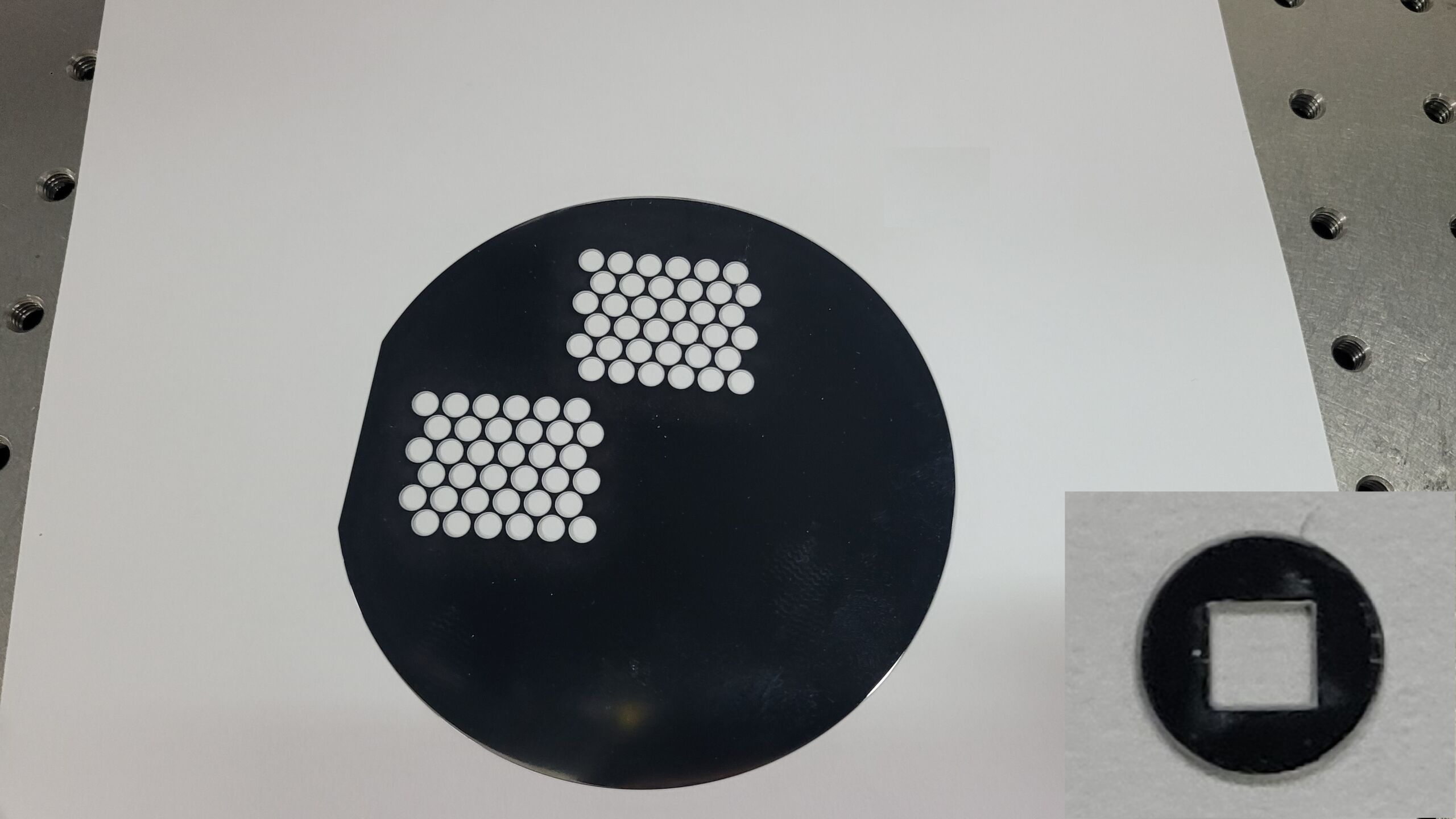
Si Wafer Pattern Cutting
Wavelength : 532nm

Si Wafer Pattern Cutting
Wavelength : 532nm
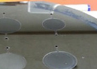
Si wafer Drilling
Wavelength : 532nm
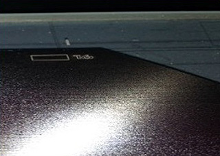
Si Wafer Align Key Marking
Wavelength : 355nm

Si Wafer Circle Cutting
Wavelength : 355nm
Thickness : 700μm
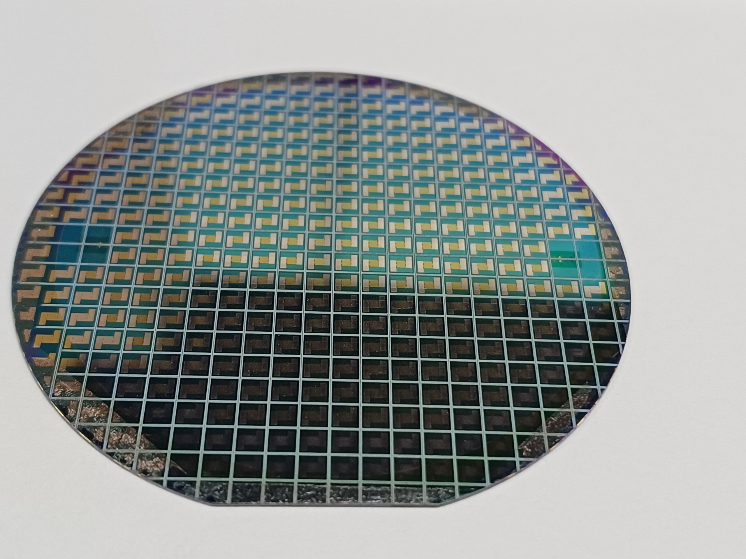
Si Wafer Pattern Cutting
Wavelength : 355nm
Ceramics
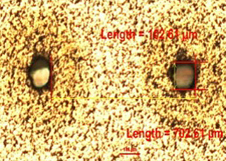
AIN Wafer Hole Drilling
Wavelength : 355nm
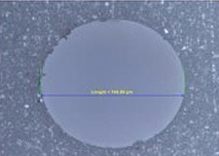
Ceramic Hole
Wavelength : 10.6μm
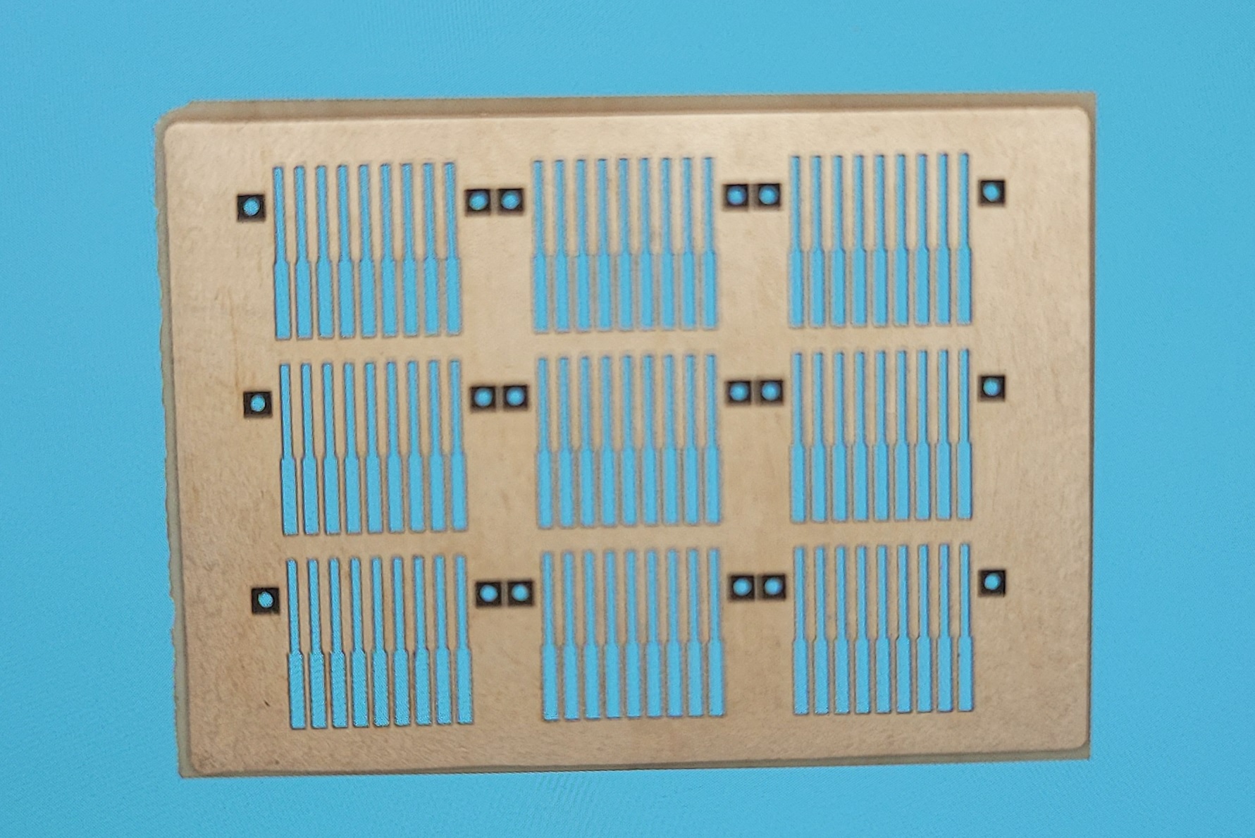
Ceramic Pattern Cutting
Wavelength : 532nm
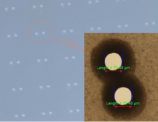
Alumina Via Hole(70μm)
Wavelength : 1064nm
Thickness : 80μm
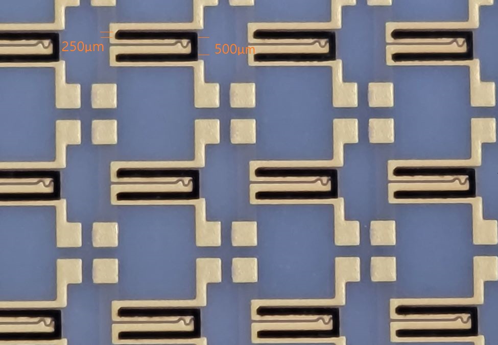
Ceramic Pattern cutting
Wavelength : 355nm
Thickness : 80μm
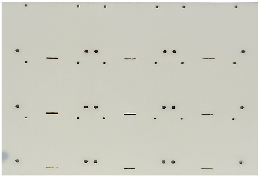
Ceramic Pattern cutting
Wavelength : 355nm(Pico seconds UV)
Thickness : 160μm
Metal
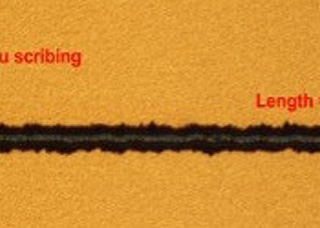
Au Pad Full Scribing
Wavelength : 355nm
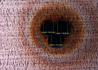
Copper Foil Hole Drilling
Wavelength : 532nm
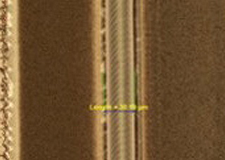
Back Electrode Film Ablation (ZnO on the Glass)
Wavelength : 355nm
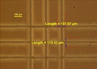
Ag Nano Wire Thin-film Scribing
Wavelength : 1064nm
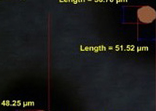
Cu Hole Drilling
Wavelength : 355nm
Thickness : 0.1mm
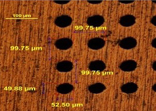
SUS Hole Drilling
Wavelength : 355nm
Thickness : 0.1mm
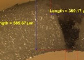
Alumina Tube Hole Drilling
Wavelength : 10.6μm
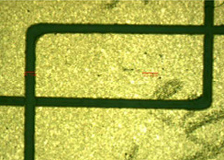
Metal Film Patterning
Wavelength : 355nm
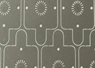
SUS304 Hole Drilling
Wavelength : 355nm
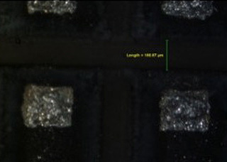
Aluminium Through Line Patterning
Wavelength : 532nm
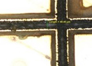
Metal Oxide Film Ablation
Wavelength : 532nm
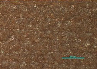
Si Wafer Metal Layer Ablation
Wavelength : 355nm
Transparent Materials & Etc.
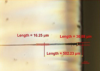
Quartz Micro-Hole Drilling (Cross-Section)
Wavelength : 355nm
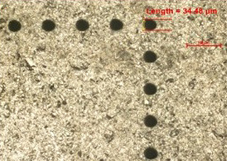
Sapphire Micro-Hole Drilling
Wavelength : 355nm
Thickness : 420μm
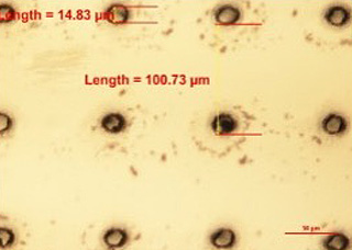
Soda-Lime Glass Hole Scribing (Via Hole)
Wavelength : 355nm
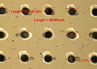
Quartz Hole Patterning (Via Hole)
Wavelength : 355nm
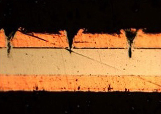
Superconductor GdBCO Thin Film Scribing (Cross-Section)
Wavelength : 355nm
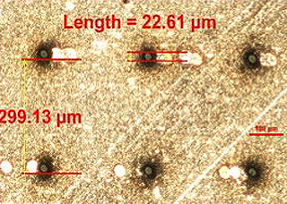
Superconductor GdBCO Thin Film Hole Drilling (Through Hole)
Wavelength : 355nm
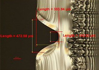
Quartz Scribing
Wavelength : 10.6μm
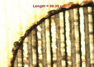
Flexible Gorilla Glass Cutting
Wavelength : 355nm

Slide Glass Cutting
Wavelength : 355nm
Glass & Medical
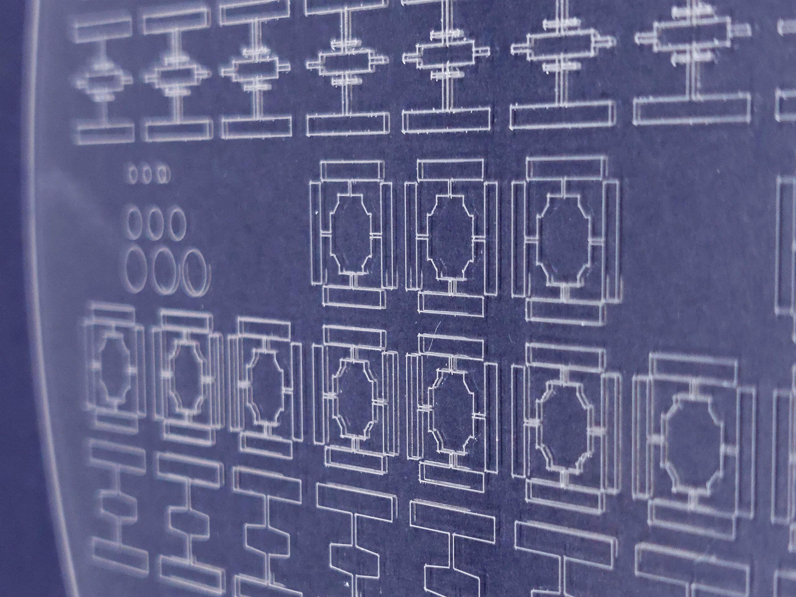
Borosilicate Glass 3.3(Dia 6", 웨이퍼)
Thickness: 1mm
Laser : Femto seconds 1030nm
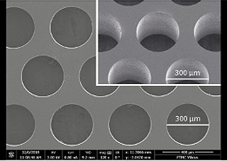
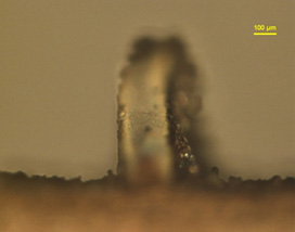
High precision glass drilling

High precision glass drilling
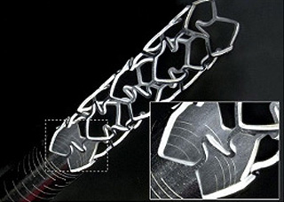
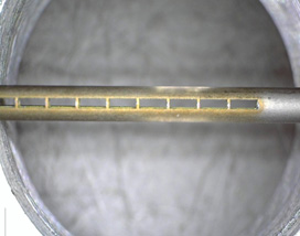
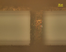
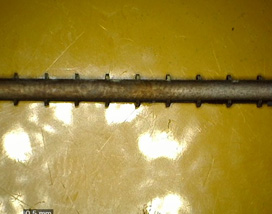
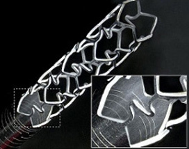
Stainless steel stent cutting
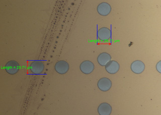
ITO Glass Top side Results
Wavelengh : 532nm
Top hat beam with pi shaper results
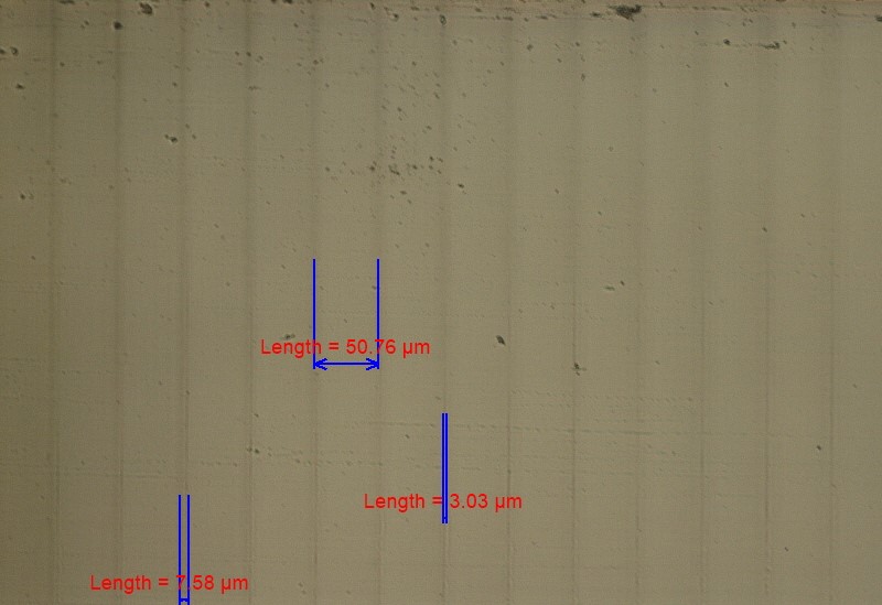
Modification Inside Glass
Wavelengh : 1064nm
Thickness : 500um
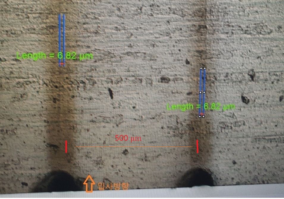
Borosilicate Glass(Bessel beam)
Wavelengh : 1030nm
Thickness : 1mm
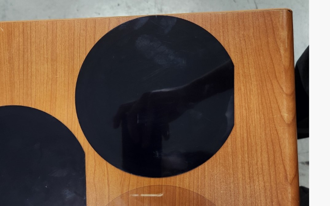
Glass 기판
Wavelengh : Femto seconds 532nm
Thickness : 600μm
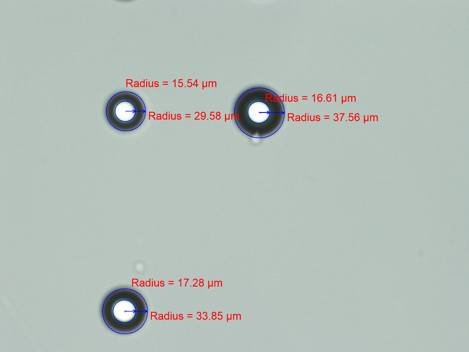
Etched TGV Substrate (D263)
Wavelengh : 1064nm
Thickness : 500um
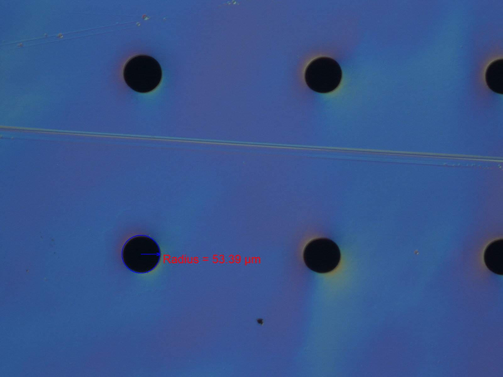
Modification TGV Substrate (D263)
Wavelengh : 1064nm
Thickness : 500um
TGV Substrate - Hour Glass Shape
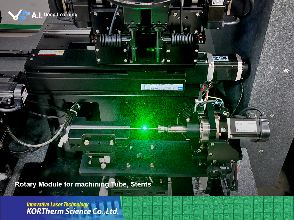
Pipe 가공 가능 Jig 구축
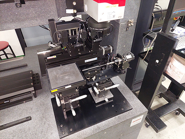
대면적 CO₂
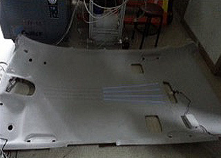
Epoxy Resin Patterning
Thickness : 355nm
기타
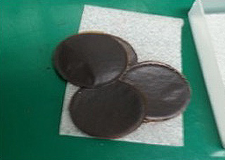
Graphene Cutting
Wavelength : 355nm
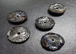
Carbon Disk Hole Drilling (100% Carbon)
Wavelength : 355nm